Silent Precision: How Ceramic Beads Are Revolutionizing the Electronics Industry
April 28, 2025
In today’s rapidly evolving electronics landscape, absolute precision is essential. As components shrink while functional requirements expand, surface quality has emerged as a critical determinant of product success. From delicate semiconductor assemblies to robust housing components, achieving flawless surfaces without compromising material integrity has become fundamental to performance, reliability, and aesthetics.
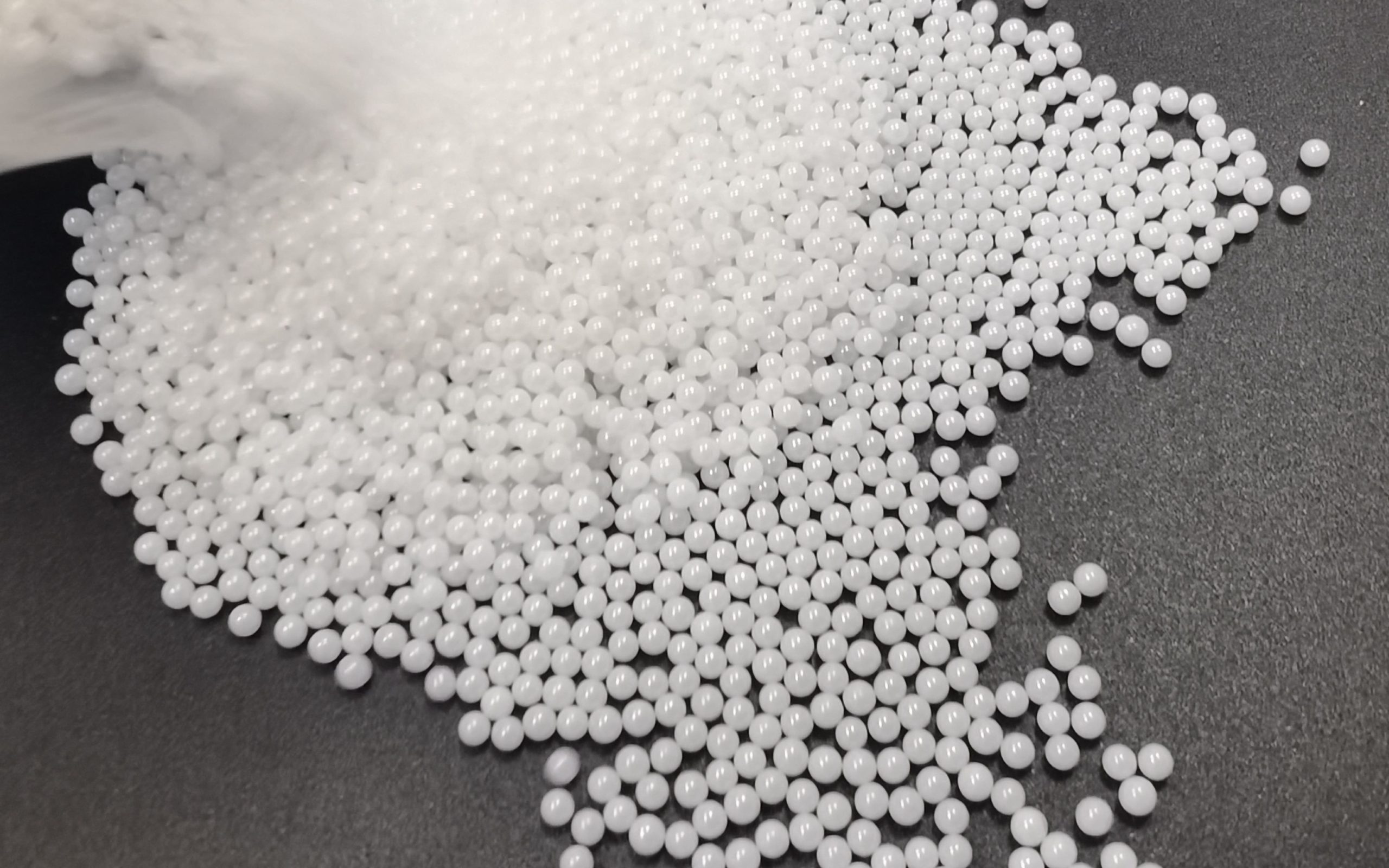
Ceramic beads have emerged as silent revolutionaries in electronics manufacturing. Unlike traditional abrasive media, ceramic beads offer a unique combination of safety, cleanliness, and precision that aligns perfectly with the uncompromising standards of today’s electronic components. This analysis explores how ceramic beads are reshaping surface treatment across the electronics sector—and why forward-thinking manufacturers are making the switch.

The Unique Surface Treatment Challenges in Modern Electronics
Electronic components present complex challenges for surface finishing and cleaning processes:
Extreme Miniaturization: Today’s components feature increasingly smaller and more fragile features that can be easily damaged by aggressive treatments.
Material Diversity and Sensitivity: Modern electronic surfaces often incorporate precious metals, specialized alloys, ultra-thin coatings, or fragile substrates requiring non-destructive cleaning.
Zero-Tolerance Contamination Risk: Even microscopic contaminants can cause catastrophic functional failures, making absolute cleanliness essential.
Exacting Precision Requirements: Surface roughness and cleanliness directly affect coating adhesion, conductivity, and long-term reliability.
Traditional abrasive methods like sandblasting with silica or steel shot can introduce micro-cracks, contamination, static charges, or leave excessive surface roughness—all unacceptable risks for high-value electronics.
Why Ceramic Beads Offer a Superior Solution
Ceramic bead blasting is rapidly becoming the method of choice for treating electronic components because it offers distinct advantages:
1. Unmatched Cleanliness and Contamination Control
Ceramic beads are chemically inert, non-metallic, and non-toxic. During blasting, they generate extremely low dust levels compared to other abrasives. This delivers key benefits:
- Minimized airborne contamination
- Reduced post-process cleaning requirements
- Enhanced process stability and consistency
- Elimination of chemical contaminants
High-quality ceramic beads maintain their integrity through hundreds of cycles, dramatically reducing fine particulate generation that could interfere with circuit functionality or coating adhesion.
2. Safe and Gentle Surface Treatment for Delicate Components
Ceramic beads, with their controlled hardness and spherical shape, impact surfaces gently without cutting or embedding into soft materials like copper, aluminum, or coated plastics.
This makes ceramic blasting ideal for numerous sensitive applications:
- PCB cleaning and preparation
- Semiconductor package surface preparation
- Connector and terminal cleaning without dimensional changes
- Selective removal of oxide layers without substrate erosion
- Treatment of components with mixed materials
3. High Precision Surface Finishing with Measurable Results
Manufactured to tight size distributions and quality standards, ceramic beads enable precise surface texturing that meets demanding engineering specifications. This precision is critical for applications where controlled roughness affects coating adhesion, solderability, or micro-assembly.
Manufacturers can tailor blasting parameters to achieve surface roughness values within extremely narrow tolerances, ensuring consistency across production batches. Advanced ceramic bead systems can achieve surface profile control with variances of less than 0.1 μm.
4. Zero Risk of Ferrous Contamination
Steel grit and other metallic abrasives pose a significant risk of embedding ferrous particles into surfaces, potentially leading to corrosion and conductivity issues. Ceramic beads, being non-ferrous and inert, eliminate these risks entirely, supporting the production of corrosion-resistant and electrically stable components.
5. Extended Media Life and Sustainability
High-quality ceramic beads demonstrate remarkable durability, allowing for 200-300 reuse cycles without significant breakdown. This exceptional longevity delivers:
- Reduced material consumption
- Minimized waste generation
- Lower operational costs despite higher initial investment
- Consistent performance throughout the media lifecycle
- Reduced equipment downtime
Real-World Applications Transforming the Electronics Sector
Ceramic bead blasting has become integral to several critical processes across electronics manufacturing:
Surface Activation Before Coating or Plating
- EMI shielding coatings on housings
- Conformal protective coatings on circuit assemblies
- Thermal interface materials on heat dissipation components
- Hydrophobic coatings on consumer electronics
The precisely controlled surface roughness improves coating adhesion while minimizing material usage and extending component lifespans.
Precision Cleaning of Post-Machining Residues
- Removal of microscopic burrs that could cause short circuits
- Cleaning of machining oils without solvent use
- Elimination of oxide layers on freshly machined surfaces
- Removal of tool marks that could create stress concentration points
Gentle Deburring of Micro-Components
- Flash removal from micro-molded plastic components
- Edge conditioning of precision-stamped metal parts
- Deburring of ceramic substrates
- Finishing of 3D-printed component housings
Aesthetic Surface Enhancement
- Uniform matte finishes on visible electronic housings
- Consistent surface texture across different materials
- Fingerprint-resistant micro-textures on touch surfaces
- Light-diffusing finishes on display surrounds
Specialized Applications in Emerging Technologies
- Semiconductor leadframes and package surfaces
- EV battery terminal connections
- Flexible electronics substrate preparation
- Optical electronics components
- Medical implantable device surfaces
In these high-value applications, the precision and cleanliness advantages of ceramic beads directly translate to improved yield rates, enhanced product reliability, and reduced warranty claims.


Future Trends: The Expanding Role of Ceramic Beads
As the electronics industry advances toward:
- Smaller, more powerful devices
- Higher integration of multi-material assemblies
- Stricter quality assurance protocols
- Greener manufacturing processes
- Increased automation and process control
The role of ceramic beads continues to expand. Advanced ceramic bead technologies include:
- Nano-structured beads with enhanced durability
- Variable-density beads for selective material treatment
- Electrically dissipative formulations
- Ultra-high-purity compositions for semiconductor applications
Integration with smart manufacturing systems enables:
- Real-time process monitoring with feedback control
- Computer vision inspection integrated with treatment systems
- Digital twin modeling for predictive quality control
- Robotic blasting systems for consistent results
Cost-Benefit Analysis: The Economic Case for Ceramic Beads
While ceramic beads represent a higher initial investment, a comprehensive analysis reveals compelling advantages:
Direct Cost Benefits
- Extended media life (15-20 times longer than glass beads)
- Reduced equipment wear (2-3 times longer nozzle and chamber life)
- Lower disposal costs
Indirect Economic Benefits
- Improved first-pass yield
- Reduced post-processing requirements
- Enhanced product performance and reduced warranty claims
- Simplified environmental compliance
For high-value electronic components, where the cost of failure far exceeds manufacturing costs, ceramic beads increasingly represent the economically rational choice.
A Quiet Revolution with Lasting Impact
In the world of electronics, where every micron matters and every contaminant can cause failure, surface preparation cannot be an afterthought. Ceramic beads offer a sophisticated solution—providing the safety, cleanliness, and precision that modern electronic manufacturing demands.
By integrating ceramic blasting into their processes, manufacturers gain strategic advantages: higher product reliability, cleaner operations, reduced environmental impact, and lower total costs. As electronics continue to pervade every aspect of modern life, the importance of component integrity will only increase.
The future of electronics is clean, precise, and dependable—and ceramic beads are helping to make that future a reality. For manufacturers committed to quality and sustainability, ceramic bead technology represents not just a process improvement but a competitive advantage in an increasingly demanding marketplace.
Filters