Electronics & Precision Manufacturing Applications – Surface Finishing Solutions
Components such as PCBs, MEMS devices, optical lenses, precision connectors, and micro-machined parts require bespoke abrasive and cleaning strategies to ensure function without compromising delicate geometries.
Introduction
Precision manufacturing and electronics combine extreme miniaturization with tight performance margins. Surface finishing in these domains is not an afterthought — it is a core enabler of reliability and yield.
The objective often moves beyond mere aesthetics: reduce particle-induced failures, remove burrs that break solder joints, improve contact conductivity, enable optical clarity, or prepare a surface for micro-adhesives.
This article provides a practical, engineering-focused reference for process selection, media choices, and measurable control criteria for electronics and precision manufacturing applications.
Key Challenges in Electronics & Precision Surface Finishing
Working at small scales introduces several unique constraints:
- Dimensional preservation: allowable dimensional change is often < ±10 μm (for many micro-machined parts) and must be strictly controlled.
- Contamination control: ionic contamination and residual particulates can cause field failures; acceptable ionic cleanliness often follows IPC-TM-650 guidance or customer-specific SIR limits.
- Thermal and mechanical sensitivity: polymeric substrates, thin metallizations, and micro-bumps are sensitive to high-impact energy and elevated temperatures.
- Complex geometries: blind vias, deep crevices, and microchannels require media and delivery systems that access tight spaces without lodging particles.
- Traceability & repeatability: production must demonstrate consistent outputs to pass qualifying audits (e.g., OEM or EMS suppliers).
Common Processes and When to Use Them
Below are the most commonly used surface finishing and cleaning processes in electronics and precision manufacturing, with recommended application scenarios.
1. Micro Deburring (Tumbling, Vibratory Finishing)
Use for: removal of machining burrs on metal connectors, stamped housings, and micro-bracket parts.
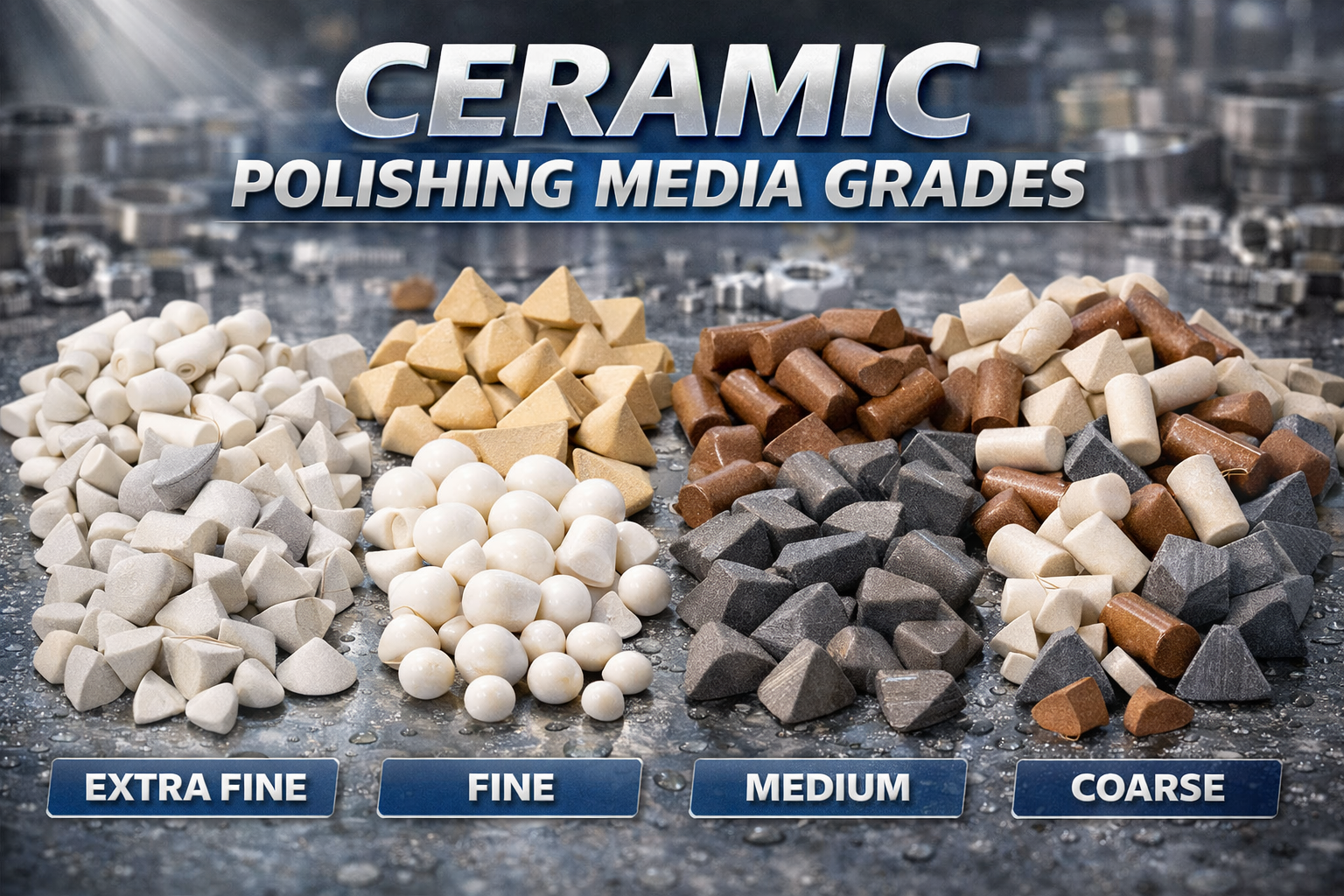
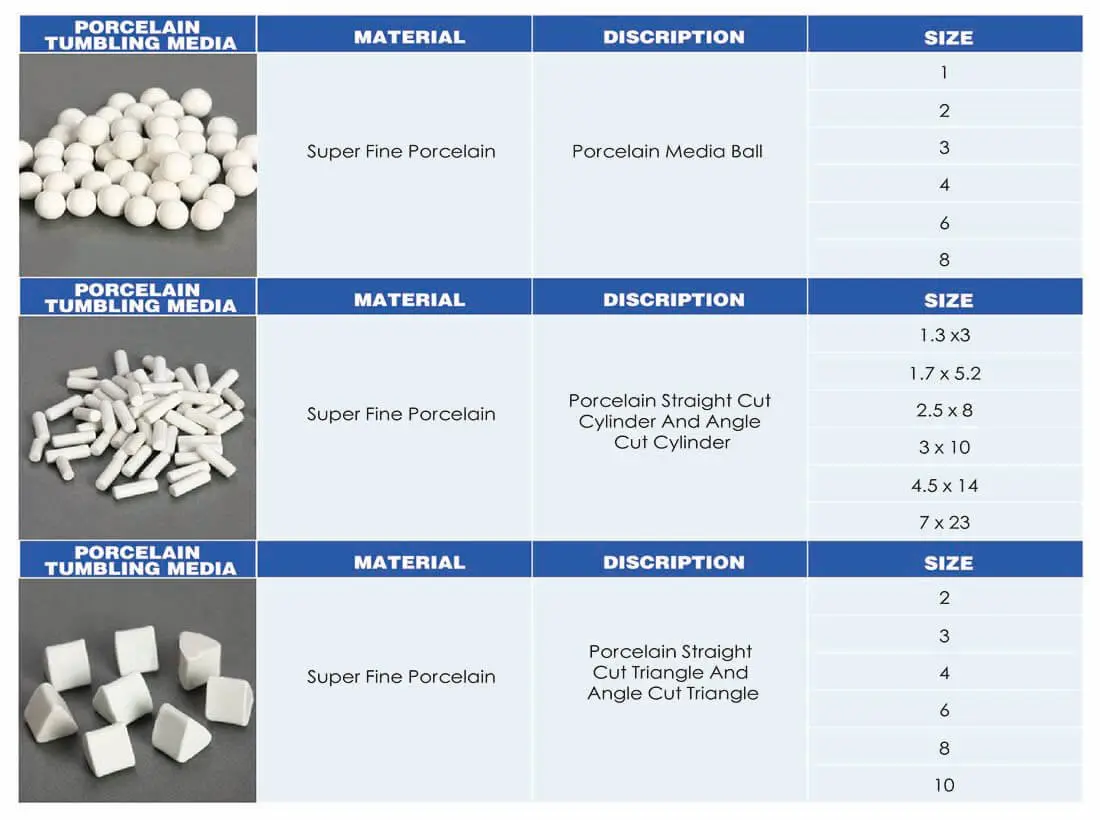
Typical media: fine ceramic pellets (0.2–1.2 mm) or engineered plastic media.
Resultado: consistent edge radius (e.g., 0.02–0.15 mm) while preserving critical dimensions.
Notas: for stamped copper or brass terminals, choose friable ceramic or soft plastic media to avoid cold-welding or excessive metal transfer.
2. Precision Polishing & Lapping
Use for: optical lenses, MEMS mirrors, and precision dies.
Methods: CMP (chemical-mechanical polishing) at sub-micron removal rates, or fine abrasive slurry lapping to reach Ra < 0.02 μm for optical-grade surfaces.
3. Low-Impact Media Blasting
Use for: removal of flash on plastic connectors, conformal coating edge definition, and soldermask smoothing.
Media: engineered plastic media (urethane, polyester) with grain sizes in the 150–600 μm range; or glass beads < 200 μm when non-cutting action is required.
Benefits: low dust, low particle embedment, and minimal thermal impact.
4. Micro Shot Peening (Selective Strengthening)
Use for: miniature springs, contact surfaces in connectors, and precision mechanical actuators requiring enhanced fatigue life.
Media: sub-mm zirconia beads or stainless steel shot with controlled Almen intensity in very low ranges (e.g., 0.002A–0.006A).
Nota: shot peening must be validated for residual stress profiles (XRD or hole-drilling methods) to ensure micro-geometry preservation.
5. Plasma, Laser & UV Cleaning
Use for: removal of organics, thin oxides, or surface activation prior to bonding. Plasma or laser cleaning provides non-contact, residue-free cleaning with minimal substrate abrasion.
Typical specs: plasma power and exposure are tuned to avoid altering polymer Tg or metal microstructure; laser fluence below damage threshold for coatings.
6. Aqueous & Solvent Ultrasonic Cleaning
Use for: particulate and flux residue removal after finishing or assembly. Ultrasonic agitation with appropriate detergents removes contaminants from blind vias and complex geometries. Critical rinsing and DI water drying follow to minimize ionic residue (target < 1 μg/cm² NaCl equiv. depending on spec).
Media Selection & Particle Size Considerations
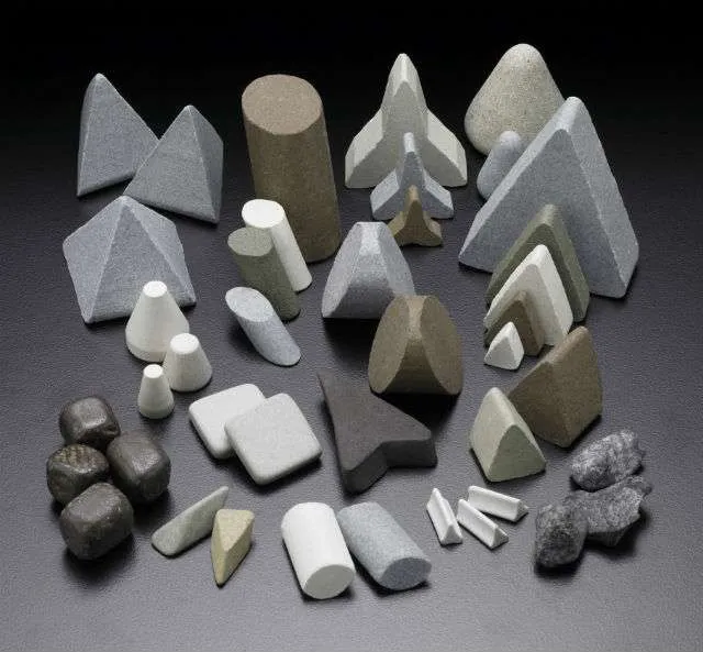
Media selection in precision manufacturing must factor in mechanical aggressiveness, shape, friability, and contamination risk. The following table summarizes practical options.
| Tipo de medio | Typical Grain/Size | Action | Aplicaciones típicas | Contamination Risk |
|---|---|---|---|---|
| Plastic Media (Urethane/Polyester) | 150–600 μm | Low-impact frictional cutting | Plastic connector flash removal, delicate metal parts | Low (non-metallic) |
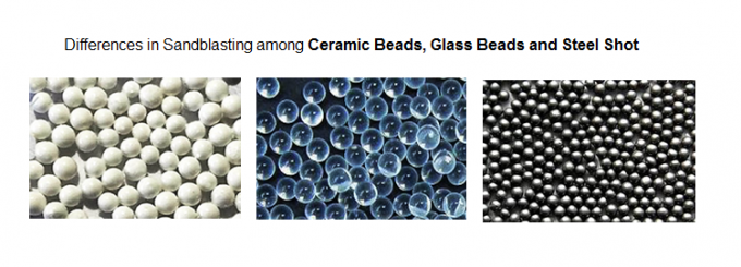
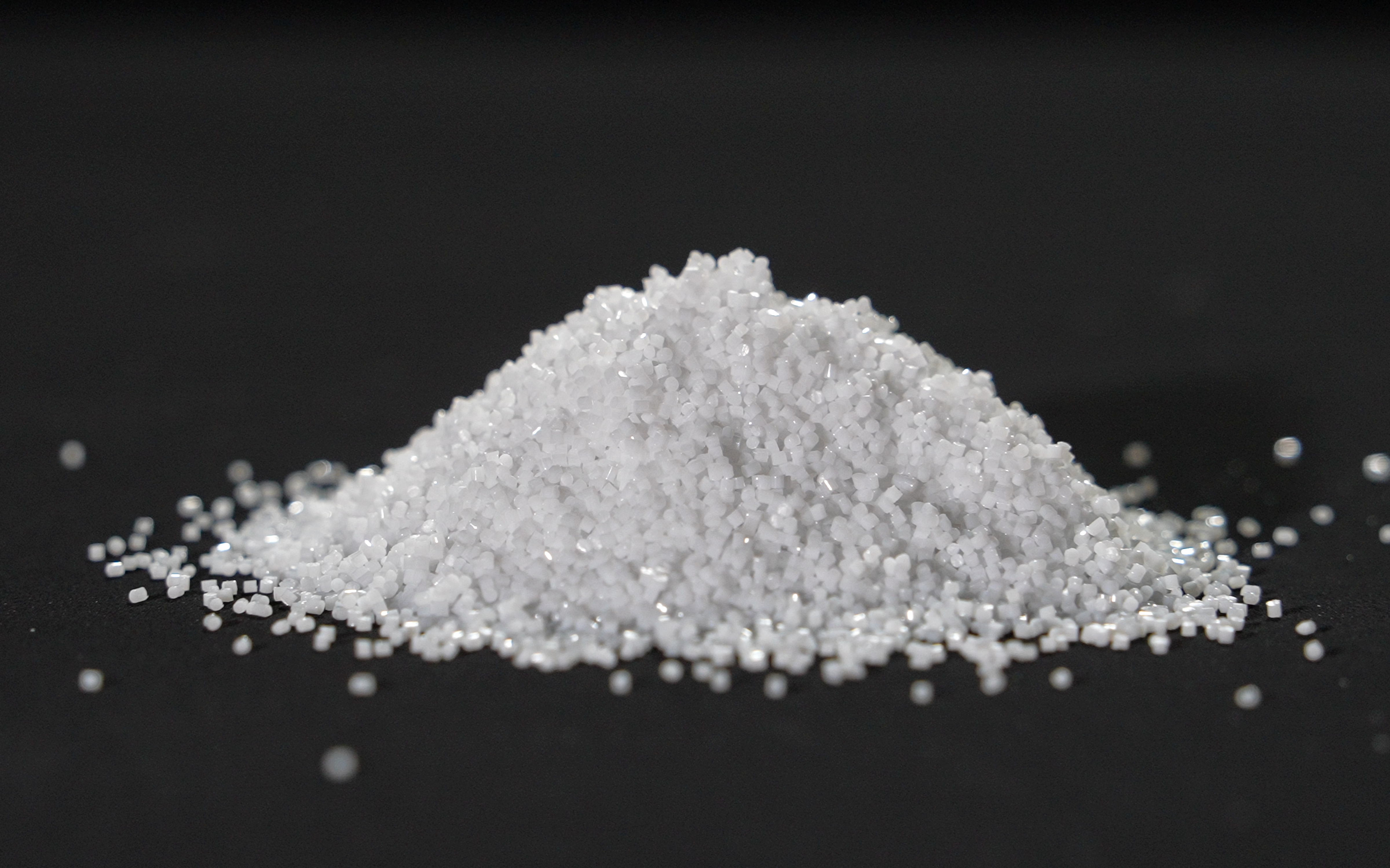
| Ceramic Micro Beads | 100–1200 μm | Slightly abrasive, uniform finish | Precision deburring, matte finishing | Moderate (non-ferrous ceramics) |
| Zirconia Micro Beads | 200–800 μm | High impact/peening | Micro shot peening of springs, contact surfaces | Low (non-ferrous, low contamination) |
| Glass Beads (Fine) | 50–250 μm | Peening/cleaning (non-cutting) | Delicate metal surfaces, coating compaction | Moderado |
| Fused Alumina (very fine) | <150 μm | Abrasive cutting | Surface prep for soldering, heavy oxide removal | Higher (angular, metal abrasion) |
Key selection rules:
- If electrical contact or conductivity is critical, avoid ferrous media or media that can embed conductive particulates in insulators.
- For optics or mirrored surfaces, use extremely fine, friable media and perform final polishing with colloidal silica to achieve Ra < 0.02 μm.
- For PCB edge and via burr removal, a combination of fine ceramic tumbling followed by ultrasonic cleaning gives the best yield with minimal damage.
Typical Process Parameters and Control Metrics
Precision processes require narrow process windows and instrumented control. The following are representative parameters used as starting points in pilot studies; actual settings must be determined by controlled experiments and validated testing.
Micro Deburring / Vibratory Tumbling (Example)
- Media: Ceramic pellets, 0.4–0.8 mm
- Compound: Neutral pH, low-foaming compound (0.5–2% by volume)
- Cycle time: 20–120 minutes depending on burr severity
- Amplitude (vibratory bowl): 0.5–2.0 mm
- Dimensional tolerance goal: < ±15 μm deviation
Low-Impact Blasting for Plastic Connectors
- Media: Engineered plastic 200–400 μm
- Air pressure: 0.2–0.5 MPa (30–75 psi)
- Nozzle distance: 80–150 mm
- Nozzle angle: 20°–60° to avoid localized overcut
- Cycle time: pulses < 5s per critical area
Micro Shot Peening
- Media: Zirconia beads 0.3–0.6 mm
- Almen intensity target (micro): 0.002A–0.006A
- Coverage: 50–120% depending on application
- Validation: XRD residual stress mapping or microhardness profiles
Ultrasonic Cleaning (Post-Finish)
- Detergent: electronics-grade, low-ionic residue
- Temperature: 25–50 °C
- Ultrasonic frequency: 25–40 kHz (higher frequencies for finer particle removal)
- Rinse: multiple DI water rinses to achieve ionic cleanliness; target TDS < 0.1 ppm
- Drying: IPA vapor or hot air with filtered dry gas to avoid stains
Monitoring metrics: particle counts after cleaning (e.g., per cm²), ionic contamination (μg NaCl/cm² equivalent), surface roughness (Ra, Rz), and dimensional variation. Feedback loops using these metrics enable continuous process control.
Case Studies
Case Study 1 — PCB Via Burr Removal and Solderability Improvement
Problema: After routing and drilling, a PCB assembly experienced micro-burrs around via holes causing solder-wicking issues and intermittent open joints.
Solución: A two-step process: (1) vibratory micro-deburring with fine ceramic media (0.25–0.6 mm) for 30–45 minutes; (2) ultrasonic aqueous cleaning with electronics-grade detergent and DI rinsing.
Resultado: Surface inspection (optical microscope, 50–200×) showed burr radius reduced to < 25 μm; solderability test (IPC-TM-650 wetting test) improved wetting time by 40%, and first-pass yield increased from 91% to 98%.
Case Study 2 — Optical Sensor Element Polishing
Problema: An IR lens used in a precision sensor had micro-scratches after molding, causing signal scatter.
Solución: Multi-stage finishing: coarse polishing with colloidal alumina slurry, followed by CMP using 50 nm colloidal silica to reach Ra < 0.01 μm and surface roughness uniformity within ±5 nm. Final cleaning used low-temperature plasma to remove organics.
Resultado: Signal-to-noise ratio improved 18%, and optical transmittance increased to design targets. Inspection by interferometry confirmed surface form deviation < λ/10 at 633 nm.
Case Study 3 — Connector Contact Surface Strengthening
Problema: Micro-springs within high-reliability connectors failed after repeated mating cycles due to micro-crack initiation.
Solución: Localized micro shot peening using zirconia beads (0.3 mm) with Almen-intensity-equivalent targets scaled to micro components (0.003A nominal). Peening performed by a micro-blast nozzle with CNC positional control.
Resultado: Fatigue cycles to failure increased by 2.3× in accelerated lifecycle testing. Electrical contact resistance remained stable; no dimensional shift beyond ±8 μm was observed.
Standards, Testing & Quality Control
Precision electronics and micro-mechanical parts often reference industry standards and test methods to demonstrate process control and cleanliness:
- IPC-TM-650 — test methods for solderability and surface cleanliness (commonly used for PCB assemblies).
- ISO 2859 / ANSI/ASQ Z1.4 — sampling plans for acceptance testing.
- ASTM E2109 — test methods for particle characterization in clean processes (applied where critical particle sizes are monitored).
- Specific customer OEM specs — many aerospace, medical, and automotive OEMs maintain stricter cleanliness and dimensional tolerance specs that supersede general standards.
Recommended QC tests: optical microscopy (50–500×), profilometry for Ra/Rz, SEM for embedded particle identification, TOF-SIMS or ion chromatography for ionic contamination, and nitration/adhesion tests where coatings follow finishing.
Practical Implementation & Cost Considerations
Implementing precision surface finishing includes piloting, scale-up, and establishing traceable QC processes. Key considerations:
- Pilot validation: run 5–25 sample parts across candidate media and parameters; capture metrics (Ra, particle counts, ionic residue).
- Process documentation: create standard operating procedures (SOPs) with defined process windows and acceptance criteria.
- Tooling & Fixturing: design fixtures that protect critical features while exposing work surfaces uniformly.
- Consumable lifecycle: track media degradation (e.g., media change when average hardness drop > 10% or when particle size distribution shifts beyond spec).
- Cost model: consider direct consumable cost, machine runtime, rework reduction, and increased yield; frequently the ROI appears within 3–9 months for high-volume production lines due to improved yield and reduced field failures.
Preguntas frecuentes
Q1: Will blasting embed media into soft polymers or PCB laminates?
A: When using engineered plastic media or low-pressure glass beads with controlled nozzle angle and distance, embedding risk is minimal. Always validate with cross-sectioning and surface elemental analysis for high-sensitivity applications.
Q2: How do I measure ionic contamination after cleaning?
A: Ionic contamination can be quantified via ion chromatography after surface extraction or by resistivity/RO water extraction per IPC-TM-650. Targets depend on product spec; many electronics assemblies aim for < 1 μg/cm² NaCl equivalent.
Q3: What is a safe air pressure range for delicate connector blasting?
A: Start at very low pressures (0.2 MPa / ~30 psi) and short pulse durations. Use fixed-distance nozzles and move the nozzle tangentially to avoid direct normal impact which concentrates energy.
Q4: How often should media be replaced or refreshed?
A: Replace media when size distribution shifts beyond ±15% of initial mean, when visual fracture increases, or when process metrics (Ra, particle capture) drift from the established control limits. Typical useful cycles vary by media: plastic media 20–40 cycles, ceramic micro beads 20–60 cycles depending on abuse level.
Call to Action
For electronics and precision manufacturing, surface finishing is a high-value lever to improve yield, reliability, and product performance. If you are evaluating finishing options for PCBs, optics, MEMS, or precision connectors, begin with a structured pilot that includes measurable acceptance criteria and traceable QC.
Filtros

