Using Plastic Media for Electronics Deflashing
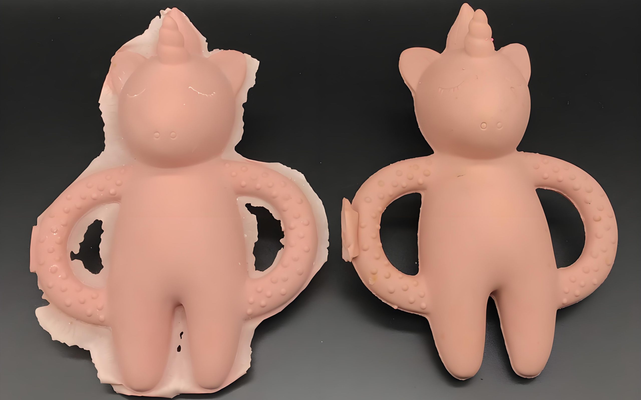
Every injection-molded electronic component — connector housings, relay cases, sensor bodies, IC package substrates, solenoid bobbins, terminal blocks — exits the mold with some amount of flash: thin films of resin that have crept into parting line gaps, ejector pin clearances, or vent slots during the injection cycle. That flash must be removed before the component can be assembled, tested, or shipped.
For most of the history of plastics manufacturing, deflashing was manual work: trained operators using hand tools, brass picks, and sharp knives to trim excess material from thousands of parts per shift. The limitations are obvious — it is slow, inconsistent, operator-dependent, and generates repetitive-strain injuries over time. It also scales badly: doubling output requires doubling the deflash labor headcount.
Plastic media blasting offers an automated, high-throughput alternative that produces more consistent results than manual deflashing while handling the geometric complexity of electronic components that other automated deflashing methods — cryogenic tumbling, vibratory finishing, laser deflashing — cannot always address effectively. For the specific package types, resin families, and quality requirements of electronic component manufacturing, understanding when and how to apply plastic media deflashing correctly is the difference between a reliable production process and a recurring quality problem.
This guide covers the complete technical picture: how flash forms and why it matters, how plastic media deflashing works, the critical decision between ambient-temperature and cryogenic processing, media selection by component type, process qualification, and the inspection standards that define success. For the broader plastic media family, see: What Is Plastic Media? The Complete Guide.
What Is Flash and Why Does It Matter?
Flash is molten resin that has escaped from the intended mold cavity into unintended areas during the injection molding cycle. It forms as a thin fin, web, or film of solidified plastic at every location where two mold surfaces meet — parting lines, ejector pin-to-sleeve interfaces, vent slot edges, slide faces, and core-to-cavity shut-off areas — wherever the clamping force, injection pressure, resin viscosity, and mold wear combine to allow a gap larger than approximately 0.0001 to 0.001 inches (depending on resin viscosity and mold temperature).
❌ What Flash Causes
- Assembly failure: Flash on connector housings prevents pin insertion or mating connector engagement — the most common functional failure mode
- Electrical short: Conductive flash bridging terminals or contact areas can create short circuits in completed assemblies
- Sealing failure: Flash on sealing surfaces prevents O-ring or gasket compression, causing leak paths in sealed housings
- Measurement error: Flash on dimensional reference surfaces causes incorrect measurements and false accepts/rejects in automated inspection
- Customer returns: Flash on cosmetic surfaces is a visual defect that triggers customer complaints and returns regardless of functional acceptability
- Downstream process interference: Flash on contact surfaces prevents reliable electrical contact in test fixtures, causing false-fail rates in production test
✅ What Complete Deflash Achieves
- Clean parting line edges with controlled, consistent edge condition matching dimensional specification
- All mold features — slots, holes, contact pockets, sealing faces — free of obstructing material
- Consistent part-to-part appearance that passes automated vision inspection without false rejects
- Predictable assembly behavior: pin insertion forces, connector mating forces, snap-fit engagement within specification
- Reliable electrical test contact on test fixture contact points
- Clean surfaces for subsequent processes: plating, coating, overmolding, adhesive bonding
How Plastic Media Deflashing Works
Plastic media deflashing uses the same fundamental mechanism as all plastic blast applications — angular polymer particles accelerated by compressed air impact the part surface — but applied to a specific engineering problem: removing thin, narrow resin projections from complex three-dimensional electronic component geometry without damaging the underlying substrate.
Flash is mechanically weaker than the surrounding part body for a precise reason: it forms in thin sections where the resin cannot pack and cool properly, creating regions with lower crystallinity (in semi-crystalline resins), higher internal stress, and smaller effective cross-section than the surrounding fully-formed wall. This geometry-based weakness differential is the physical basis for selective flash removal — the flash fractures under impact stress before the part body does, because the flash has a fundamentally unfavorable ratio of load-bearing cross-section to applied force.
The operator’s task in process qualification is to find the parameter window where this differential is maximized: where flash removal is complete, fast, and consistent, and where no abrasive damage to part body surfaces, conductor traces, or dimensional features occurs. For electronic components — which have extremely fine features, tight tolerances, and functional surfaces that cannot tolerate any material removal — this window is typically narrow, and finding and holding it requires careful qualification work.
For ambient-temperature deflashing: The part is at room temperature during blasting. The resin’s flash must be brittle enough at ambient temperature to fracture under blast impact before the part body deforms. This works reliably for thermoset resins (epoxy molding compounds, phenolic) and for thermoplastics that are rigid and brittle at room temperature (PS, SAN, some grades of PBT and LCP). For thermoplastics that remain flexible at room temperature (PA, PP, TPE-based compounds), ambient deflashing often produces incomplete removal — the flash bends under each impact rather than fracturing — making cryogenic processing necessary.
For cryogenic deflashing: The parts are cooled to below the glass transition temperature (Tg) or brittle transition temperature of the specific resin before blasting. Below this temperature, the flash becomes brittle — it fractures cleanly under low-energy blast impact — while the part body, being thicker, retains enough thermal mass to remain above its damage threshold during the brief blast cycle. The physical state change from flexible to brittle is the mechanism that makes selective flash removal possible on thermoplastic materials that cannot be reliably deflashed at ambient temperature.
Deflashing Methods Compared
- High throughput (batch)
- Consistent part-to-part
- Complex geometry access
- Ambient or cryo
- Low per-part cost
- Requires qualification
- Media reclaim possible
- Best for: connectors, housings, sensor bodies, IC packages
- No blast media needed
- Very gentle on substrate
- Limited geometry access (no internal features)
- Requires cryo system
- Slower throughput
- Inconsistent on thick flash
- No directional control
- Best for: simple shapes, rubber, soft TPE
- Zero equipment cost
- Flexible for any geometry
- Very slow (labor intensive)
- High variability
- Operator fatigue risk
- RSI / ergonomic issues
- Cannot scale efficiently
- Best for: prototypes, very low volume
- Sub-millimeter precision
- No media contamination
- Extremely high capital cost
- Slow throughput per part
- Limited to accessible surfaces
- Heat-affected zone risk
- Best for: ultra-fine features, BGA, CSP packages
- Reaches all surfaces
- Slow process (hours)
- Hazardous waste stream
- Risk of residue
- May attack metallic leads
- Compatibility testing required
- Best for: thermoset encapsulants with solvent-soluble flash only
Plastic media blasting occupies the optimal position for most high-volume electronic component deflashing: it handles complex three-dimensional geometry that cryogenic tumbling alone cannot reach, processes parts in batches that manual trimming cannot match for throughput, and operates at a capital and per-part cost far below laser deflashing. The qualification requirement is the primary barrier to implementation — but for any program producing more than approximately 50,000 parts per year, the qualification investment is recovered in labor savings within weeks.
Ambient vs Cryogenic Deflashing: Choosing Correctly
The ambient vs. cryogenic decision is the most consequential process choice in plastic media deflashing for electronic components, and the one that trips up operators who carry assumptions from other blast applications. The decision is driven by the resin’s mechanical properties at room temperature — specifically whether the flash is brittle enough at ambient temperature to fracture cleanly under blast impact.
| Decision Factor | → Use Ambient Deflashing | → Use Cryogenic Deflashing |
|---|---|---|
| Resin type | Thermoset epoxy, phenolic, DAP; rigid amorphous thermoplastics (PS, SAN) | Flexible thermoplastics: PA (nylon), PP, TPE, TPU, PBT, soft PVC |
| Flash thickness | Very thin (<0.1 mm) — tears rather than deforms under blast | Any thickness flexible flash — needs embrittlement regardless of thickness |
| Flash behavior test | Flash snaps cleanly when bent sharply at room temperature | Flash bends without breaking at room temperature — will not respond to ambient blast |
| Component sensitivity | Metal leads, fine pitch — need lowest possible blast energy (ambient + very low PSI) | Robust housing — cryo embrittlement allows lower effective blast energy on thick flash |
| Production throughput | Faster cycle — no cooling time required | Slower cycle — cooling adds 5–20 minutes per batch; must manage temperature recovery |
| Equipment investment | Blast cabinet only (lower capital) | Cryogenic system + blast cabinet (higher capital; liquid nitrogen supply required) |
| Operating cost | Lower — no cryogen consumption | Higher — liquid nitrogen cost adds $0.005–$0.05/part depending on batch size |
The Bend Test: Quick Field Determination
If you are unsure which approach is appropriate for a specific resin, the simplest field test is the bend test: take a representative flash thin section from a production part and try to snap it with your fingers at room temperature. If it snaps cleanly with a brittle fracture — ambient deflashing will work. If it bends or deforms plastically without breaking — cryogenic processing is required. This test takes 10 seconds and gives you the correct process direction before any equipment setup or qualification work begins.
Cryogenic Deflashing: The Process in Detail
Cryogenic deflashing combines controlled temperature reduction to below the resin’s brittle transition point with plastic media blast impact to achieve clean, complete flash removal on thermoplastic components that cannot be deflashed at ambient temperature. The key to successful cryogenic deflashing is precise temperature management — too warm and the flash remains flexible; too cold and the part body itself becomes brittle enough to crack under impact.
Temperature Selection by Resin
| Harz | Typical Brittle Transition | Target Cryo Temp | Soak Time | Notes |
|---|---|---|---|---|
| PA66 (Nylon 66) | -4°F to -22°F (-20°C to -30°C) | -40°F to -60°F | 5–8 min | Moisture content affects transition temp; dry-as-molded vs. conditioned PA behaves differently |
| PA6 (Nylon 6) | 14°F to -4°F (-10°C to -20°C) | -30°F to -50°F | 5–8 min | Slightly higher transition temp than PA66; less aggressive cryo required |
| PP (Polypropylene) | 14°F to 32°F (-10°C to 0°C) | -20°F to -40°F | 4–6 min | Wide variation by grade; homo-PP more brittle at lower temperatures than co-PP |
| PBT (Polybutylene Terephthalate) | 32°F to 50°F (0°C to 10°C) | -20°F to -40°F | 4–6 min | Often used unfilled in connectors; glass-filled grades deflash more easily (glass increases brittleness) |
| PET (Polyethylene Terephthalate) | 41°F to 59°F (5°C to 15°C) | -20°F to -30°F | 4–6 min | Common in bobbins and coil formers; deflashes reliably with moderate cryo |
| LCP (Liquid Crystal Polymer) | Ambient — inherently brittle | Ambient (no cryo needed) | — | LCP is inherently brittle at room temperature; ambient deflashing at very low pressure (8–15 PSI) |
| PPS (Polyphenylene Sulfide) | Ambient — inherently brittle | Ambient (no cryo needed) | — | High-temperature thermoset-like behavior; ambient deflashing at low to moderate pressure |
| TPE / TPU | -40°F to -80°F (-40°C to -62°C) | -60°F to -100°F | 8–15 min | Most difficult; wide grade variation. Test each compound individually — some TPEs resist embrittlement even at extreme cryo temperatures |
| Epoxy Molding Compound (thermoset) | Ambient — thermoset is brittle | Ambient (no cryo needed) | — | Standard IC package encapsulant; ambient deflashing is appropriate and preferred |
Media Selection for Electronic Components
For electronics deflashing, Type V acrylic (PMMA) is the default media selection in virtually all cases. The reasoning is direct: electronic components contain embedded metal conductors, fine features, and dimensional interfaces that cannot tolerate any abrasive damage. Type V acrylic’s lower hardness, lower density, and thermoplastic deformation behavior produce the lowest substrate impact stress of any plastic blast media — and in deflashing applications where the substrate damage threshold is narrow, that minimum effective impact energy is the correct starting point.
Type II urea (fine grade, Mesh 50–60) is sometimes used for ambient deflashing of robust thermoset components — specifically epoxy-encapsulated IC packages being deflashed at ambient temperature, where the thermoset material provides a harder, more damage-resistant substrate than thermoplastic housings. Even in these cases, qualify with Type V acrylic first and move to fine Type II urea only if acrylic cannot achieve adequate flash removal within the substrate damage window.
| Component / Application | Medienart | Mesh | Prozess | Grund |
|---|---|---|---|---|
| Epoxy-encapsulated IC packages (DIP, SOP, QFP) | Type V Acrylic | 60–80 | Ambient | Thermoset brittle at ambient; fine mesh protects exposed lead frame |
| Connector housings (PA66, PA6) | Type V Acrylic | 50–60 | Cryogenic | PA is flexible at ambient; cryo required; acrylic minimizes conductor damage risk |
| Connector housings (LCP, PPS) | Type V Acrylic | 60–80 | Ambient | LCP/PPS inherently brittle; finest mesh protects fine-pitch contact features |
| Relay cases and bobbins (PBT, PET) | Type V Acrylic | 50–60 | Cryo or ambient | Test resin grade; PBT may deflash ambient; PET usually requires moderate cryo |
| Sensor housings (PP, PE) | Type V Acrylic | 50–60 | Cryogenic | PP is flexible at ambient; cryo essential; robust housing allows slightly coarser mesh |
| Solenoid bobbins (phenolic, DAP) | Type V Acrylic oder Fine Type II | 50–60 | Ambient | Thermoset — brittle at ambient; more robust substrate allows fine Type II if needed for heavier flash |
| TPE / TPU components | Type V Acrylic | 60–80 | Deep cryogenic | Requires deepest cryo temperature; finest mesh at absolute minimum pressure; test thoroughly |
| Terminal blocks (PA or PBT) | Type V Acrylic | 50–60 | Cryo or ambient | Metal inserts require conductor protection; acrylic minimizes risk of insert damage |
Package Type Guide: Parameters by Component
Resin Compatibility Matrix
Operating Parameters Reference
Process Qualification: Step by Step
Characterize the Flash and the Component
Before selecting any parameter, document the flash completely: measure its thickness at multiple locations using a calibrated optical micrometer or SEM cross-section (typical electronic component flash is 0.01–0.3 mm thick). Identify the resin grade from the material data sheet — not just the family (PA66) but the specific grade and filler content, which affects brittle transition temperature. Map all functional surfaces on the component that must be protected: contact areas, sealing faces, fine pitch leads, dimensional datums. Photograph sample parts under 10× magnification with consistent lighting to establish a visual baseline.
Request the specific resin data sheet from the molder, not just the trade name. PA66 grades from different suppliers can have brittle transition temperatures varying by 30–50°F — this directly affects the cryogenic temperature setting needed.
Determine Process Type: Ambient or Cryogenic
Perform the bend test on representative flash sections at room temperature. If flash snaps at ambient: proceed to ambient qualification. If flash bends: cryogenic processing is required. For grade-dependent resins, also perform a second bend test after cooling the flash sample to -40°F — if it then snaps, that temperature is at least at the lower bound of the target cryogenic range. If it still does not snap at -40°F, a colder target temperature is needed, or the resin may be resistant to cryogenic embrittlement (some highly rubber-toughened grades resist embrittlement even at very low temperatures).
Initial Parameter Set Selection
Select starting parameters at the conservative end of the applicable range: Type V Acrylic, finest appropriate mesh for the component’s lead pitch or feature size, and pressure at the lower bound (8–12 PSI for fine-pitch IC packages; 12–15 PSI for connector housings). For cryogenic processes, target a temperature 20–30°F below the brittle transition point of the flash material — this provides margin for temperature variation across the batch.
Trial Blast on Qualification Sample
Blast five qualification components at the initial parameter set. After each blast cycle, inspect under 10× optical magnification: check for flash removal completeness in all locations, check for any abrasive damage to functional surfaces (lead deformation, contact area abrasion, dimensional feature alteration). If flash is incompletely removed: increase either pass count (preferred) or pressure (secondary). If substrate damage is observed: reduce pressure immediately and do not proceed with the current parameters. Document every trial step with photographs and measurements.
Run the electrical continuity test on qualification samples immediately after deflash inspection. Deflash-induced subtle lead distortion that passes visual inspection may still cause marginal contact force changes that show up as borderline continuity test results.
Functional Testing of Qualified Samples
Submit 10–20 qualification samples to all downstream functional tests that could reveal deflash-induced defects: electrical continuity, mating force measurement (for connectors), seal test (for sealed housings), lead coplanarity (for IC packages), dimensional measurement of critical features. These tests confirm that the parameter set achieves complete flash removal without functional degradation — passing visual inspection alone is insufficient for qualification of electronic components.
Process Window Validation and Documentation
Run a process window validation study at the qualified parameters: blast three separate batches at the nominal parameters, at +5 PSI above nominal, and at -5 PSI below nominal. The nominal parameters must achieve full flash removal; the -5 PSI condition confirms the lower-bound behavior (incomplete flash removal defines the lower limit); the +5 PSI condition must not produce any substrate damage (damage appearance defines the upper limit). Document the qualified parameter set — media type, mesh size, pressure, blast time, nozzle bore, cryogenic temperature and soak time if applicable — in a formal process specification. This document is the production control reference.
Fixturing and Part Protection
Fixturing is disproportionately important in electronics deflashing compared to other blast applications because electronic components are small, fragile, and contain features that must be protected from direct blast impact. The difference between a correctly fixtured component and an incorrectly held part can be the difference between a reliable production process and a chronic lead-damage problem.
Why Fixturing Matters for Electronic Components
Without fixturing, loose parts in a blast chamber move under the blast stream, presenting random surfaces to the nozzle rather than presenting flash locations consistently. This produces variable flash removal (some areas thoroughly cleaned, others missed entirely) and creates part-on-part collision damage as parts tumble against each other under blast pressure. For electronic components with fine-pitch leads, a single inter-part collision during blasting can bend multiple leads simultaneously — producing a reject rate that appears to be a deflash parameter problem but is actually a fixturing problem.
Fixturing Options by Component Type
| Component Type | Fixturing Approach | Key Protection Requirements |
|---|---|---|
| IC packages (DIP, SOP, QFP) | Custom aluminum carrier trays with individual part pockets that orient the component with leads protected — only the package body parting line exposed to blast stream. Automated nozzle sweep across tray surface. | Leads must be recessed below the carrier tray surface or supported laterally. Nozzle sweep angle must never direct blast parallel to lead row direction. |
| Connector housings (bulk, non-fine-pitch) | Perforated basket or mesh drum for rotating batch blast. Parts load loosely with sufficient media-to-part ratio (min 3:1) to prevent part-on-part contact. Manual inspection of first batch for part-on-part marks before production. | Contact pocket openings should face blast stream direction for maximum cleaning access. Remove any loose insert components before batch blast. |
| Fine-pitch connectors | Individual strip carriers or molded trays that locate each connector at fixed orientation. Automated indexed nozzle sweep — not batch tumble. | Contact entry faces must be fully exposed to blast; mating face must be protected from direct blast impact. |
| Solenoid bobbins / cylindrical parts | Spindle fixturing that rotates part during blast cycle, ensuring uniform coverage of cylindrical parting lines. Or racked trays with consistent angular orientation. | Wound coil wire (if present) must be protected from direct blast with masking plug or removed before blast and re-installed after. |
| Terminal blocks / multi-insert parts | Individual fixturing that exposes wire entry slots and terminal holes to blast while protecting underside. Manual pre-check that all metal inserts are fully seated before blasting. | Verify all insert positions before and after blast — blast energy can shift loosely seated inserts. |
Post-Deflash Inspection Standards
Inspection after electronics deflashing must cover both flash removal completeness and the absence of deflash-induced damage. Visual inspection alone is insufficient for most electronic component qualification — functional tests are required to confirm that the deflash process has not introduced subtle damage that escapes visual detection.
- Parting line edges clean — no visible flash film under 10× magnification at any location
- All functional openings (contact pockets, wire entry, mounting holes) fully clear of obstructing material
- Lead geometry unchanged — pitch, coplanarity, and form within specification
- Package body surfaces free of abrasive scoring, surface whitening, or material removal marks
- Metal contacts and lead frames free of abrasive damage, pitting, or deformation
- Sealing faces clean and dimensionally intact (measured with gauging if seal is functional requirement)
- Electrical continuity within specification on all qualified test points
- Assembly force (pin insertion, mating engagement) within specified range on sample set
- Any residual flash film visible at 10× at any location — classify as incomplete deflash, return for re-process
- Lead deformation, bending, or pitch change beyond specification — dimensional damage, stop production
- Surface abrasion marks on lead frame or contact area — media damage, reduce pressure immediately
- Package surface crazing, whitening, or micro-cracking — over-blasting or incorrect parameters, stop and re-qualify
- Loose or displaced metal inserts — fixturing or parameter issue, investigate before continuing
- Electrical continuity failure on any qualified test point — functional damage, stop production, escalate
- Assembly force out of specification on sample — investigate contact geometry and flash removal completeness
- Contamination: media particles visible in contact pockets or lead clearances — blow-out deficiency, rework blow-out protocol
Inspection Frequency
For production deflashing of electronic components, the minimum recommended inspection protocol is: 100% visual at 5–10× magnification for first article and after any process parameter change; statistical sampling (AQL 1.0 or stricter) for visual inspection in steady-state production; periodic functional testing (electrical continuity, mating force) on a defined sample size per lot. For safety-critical applications (automotive electronics, medical device components), 100% electrical functional test after deflashing is typically required by the quality system regardless of visual inspection results.
Troubleshooting Guide
Flash is not being removed — parts look the same before and after blast
This is the most common deflashing failure mode in electronics. A thermoplastic flash that bends under blast impact absorbs the energy elastically and springs back — it cannot be removed by ambient blast regardless of how high the pressure is raised. Raising pressure in an attempt to overcome flexibility will damage the part body before it ever removes the flash. Confirm resin flexibility with the bend test and convert to cryogenic processing if the flash does not snap cleanly at ambient temperature.
Cryogenic deflash produces incomplete removal — flash remains flexible after cooling
Not all resins of the same family respond to cryogenic embrittlement at the same temperature. A PA66 with 15% rubber toughener has a significantly lower brittle transition temperature than an unfilled PA66. Reduce the cryogenic target temperature in 10°F increments and re-test. If the flash still does not embrittle at -100°F, the resin may be specifically formulated to resist low-temperature brittleness — consult the material supplier for the specific brittle transition temperature of that exact grade. Some highly elastomeric grades simply cannot be deflashed by any blast method and require laser or manual trimming.
Lead deformation on IC packages — leads bent or pushed out of plane
Lead deformation is the most serious deflash damage mode for IC packages. The three most common causes are: (1) blast pressure above what the lead cross-section can resist — reduce by 3 PSI and re-evaluate; (2) nozzle sweep direction parallel to the lead row, which creates a drag force along the lead length rather than an impingement force on the flash — always blast perpendicular to lead rows; (3) parts tumbling against each other in batch blast operation — increase media-to-part ratio to 5:1 minimum, or switch to individual part fixturing on carrier trays.
Inconsistent results — some parts fully deflashed, others not
Part-to-part inconsistency in batch deflashing usually has one of three root causes. First, nozzle sweep pattern gaps — areas of the blast field where media density is lower, producing under-blasted parts in those zones. Map the blast pattern by blasting a flat sheet of construction paper and verifying uniform media distribution across the blast zone before processing parts. Second, cryogenic temperature non-uniformity — parts at the top of a deep batch load may not cool as thoroughly as those at the bottom, warming through their brittle transition during the blast cycle. Reduce batch depth or verify that the cryogenic system provides uniform temperature throughout the load. Third, moisture-contaminated media — wet media clumps and flows inconsistently, producing blast density variation across the cycle.
Media contamination in part features — white particles visible inside contact pockets
Media particles trapped in functional features of electronic components are a direct quality defect — they interfere with pin insertion, create false electrical contact, and can dislodge during field use causing intermittent failures. The first response is always to improve the post-blast blow-out protocol: increase blow-out air pressure to 80–100 PSI, use a fan nozzle that sweeps the entire component, and ensure the blow-out is performed with the component oriented so that gravity assists media ejection from pocket features. For electrostatically charged components (common with LCP and PPS), a brief anti-static treatment (ionized air bar) before blow-out breaks the static bond that retains media particles. If a specific pocket geometry consistently traps media regardless of blow-out protocol, redesign the fixturing to orient that feature upward during blow-out.
Critical Mistakes to Avoid
1. Not Performing the Bend Test Before Process Selection
Assuming that all plastic parts can be deflashed at ambient temperature — without testing the specific resin’s flexibility — is the root cause of the majority of electronics deflashing process failures. Five seconds with a piece of flash material and your fingers determines whether you need a cryogenic system or a simple blast cabinet. Skipping this test wastes qualification time on an approach that will never work for flexible thermoplastics.
2. Starting Qualification at High Pressure to Save Time
The instinct to “find the right parameters quickly” by starting at medium-high pressure and reducing if damage occurs is exactly backwards for electronic components. At high pressure, lead deformation, surface abrasion, and contact damage can occur in the very first qualification blast — on a batch of parts that cannot be recovered. Always start at minimum and work upward. The qualification time difference between starting low vs. starting high is measured in hours; the cost difference between a qualification batch that shows no damage vs. one that destroys samples is measured in recovery time and engineering escalation cycles.
3. Qualifying on One Lot and Assuming Universality
Flash characteristics vary with mold wear, resin lot variation, and process parameter drift at the molder. A qualification performed on a fresh mold with new-lot resin may not hold when the same program runs with a worn mold or slightly different resin. Build process monitoring into the production protocol — periodic first-article deflash checks after mold PM at the molder, or when resin lots change, confirm that the qualified parameters still produce acceptable results on current production parts.
4. Blasting Metal-Exposed Lead Frames at Ambient Parameters Without Lead Geometry Verification
Lead coplanarity (the flatness of a set of package leads relative to the mounting plane) is a critical solderability specification for IC packages. Even minor blast-induced lead deformation that passes visual inspection at 10× can shift coplanarity beyond IPC-7711 limits, causing solder joint failure in reflow. Add lead coplanarity measurement to the qualification acceptance criteria for any package type where coplanarity is a solderability specification, not just to the visual inspection protocol.
5. Omitting the Post-Blast Blow-Out Step
The post-blast blow-out step — thorough compressed air cleaning to remove all media particles and flash debris from part surfaces and internal features — is treated as optional by some operators and is the direct cause of media-contamination field returns when omitted. It is not optional. For electronic components going into automated assembly, a single media particle trapped in a terminal entry or contact pocket causes a machine jam, a false electrical test failure, or a field assembly defect. The blow-out step costs 5–10 seconds per batch and prevents a category of defect that can cost orders of magnitude more to address downstream.
Häufig gestellte Fragen
Can plastic media deflashing be used on assembled PCBs or modules, not just individual components?
Plastic media blasting is generally not appropriate for assembled PCBs or completed electronic modules. The concern is not the blast media’s effect on the PCB substrate — FR4 laminate is reasonably compatible with plastic blast at low pressure — but the risk to surface-mounted components: exposed capacitor and resistor terminations can be abraded, fine-pitch IC package leads can be deflected, and solder joints can be stressed by the blast impact energy. For cleaning of assembled boards (flux residue removal, conformal coating stripping), specialized processes like CO₂ snow cleaning, aqueous cleaning with spray nozzles, or plasma cleaning are more appropriate. Plastic media blast deflashing is specifically a pre-assembly process applied to individual molded components before they carry any electrical components, solder joints, or circuit elements.
How do I deflash components with exposed bare copper or tin-plated leads without damaging the plating?
Lead plating protection is one of the most critical concerns in IC package deflashing. The approach is threefold: first, use the finest available mesh (Mesh 80) and lowest effective pressure (starting at 8–10 PSI) to minimize abrasive contact force on exposed plated surfaces. Second, orient the component in fixturing so that the blast stream approaches the package body’s parting line at an oblique angle rather than directly impacting lead surfaces — ideally, the leads should be in the blast shadow of the package body, with the flash on the package body parting line in direct line of sight. Third, inspect plating integrity post-blast with a 4-point probe or tin whisker inspection protocol depending on the plating specification. Note that lead-free tin plating is softer than lead-tin alloy plating and requires more conservative parameters. If plating damage persists at minimum parameters with optimal fixturing, laser deflashing is the appropriate alternative for that specific package configuration.
What is the throughput of a production plastic media deflashing system for small electronic components?
Throughput varies significantly by component size, fixturing approach, and whether cryogenic processing is required. For ambient deflashing of small connectors or IC packages using carrier tray fixturing and automated nozzle sweep, a dedicated deflashing system can typically process 500–2,000 parts per hour depending on tray capacity and blast cycle time. For cryogenic deflashing, the cooling and soak cycle adds 10–25 minutes per batch, which reduces effective throughput to 200–800 parts per hour depending on batch size. High-volume dedicated deflashing equipment (drum-style rotary blast systems with integrated cryo and media reclaim) can achieve throughputs of 1,000–5,000 small parts per hour in sustained operation. For comparison, manual deflashing of the same small connectors by hand typically achieves 100–300 parts per operator-hour, making automated plastic media deflashing 3–15× faster per labor unit for most electronic component geometries.
Does cryogenic treatment affect the mechanical or electrical properties of electronic components permanently?
For properly designed cryogenic deflashing processes, the answer is no — the cryogenic treatment does not permanently alter the mechanical or electrical properties of the components. The cooling is a reversible physical state change: the resin embrittles at low temperature and recovers its normal mechanical properties fully as it warms back to ambient temperature. For metal lead frames and contacts, the cryogenic temperatures used in deflashing (-40°F to -100°F) are within the normal operating temperature range of most electronic components and do not cause any metallurgical change to copper alloys or standard plating materials. The one potential concern is for components with pre-existing internal stress concentrations (from injection molding) or micro-cracks — rapid cooling can propagate these into visible cracks. This is why the qualification process requires inspection of multiple batches of thermally cycled parts, not just the first trial, to detect any latent thermal cycling sensitivity before the process enters production.
Is there a minimum flash thickness below which plastic media deflashing is not effective?
For thermoset and brittle thermoplastic materials, plastic media deflashing is effective on flash as thin as 0.01–0.02 mm (10–20 µm) — essentially any flash that has enough structural thickness to constitute a physical projection from the part surface. Very thin flash on brittle resins actually tends to be easier to remove than thicker flash because the thinner section fractures at lower impact energies. For flexible thermoplastic materials, even very thin flash (0.05 mm) can require cryogenic processing because the issue is material flexibility, not section thickness — a 0.05 mm film of PA66 at room temperature is flexible regardless of its thinness. The practical lower bound for effective cryogenic deflashing is approximately 0.01–0.02 mm of flash thickness — below this, the flash is so thin that it may not be mechanically significant (it may be acceptable by specification) or may not represent enough material to fracture selectively from the part body even under cryogenic conditions. Flash below this threshold is typically addressed by optimizing the mold rather than by post-mold deflashing.
Filter


")


")